ΕΡΓΑΣΤΗΡΙΟ ΨΗΦΙΑΚΩΝ ΣΥΣΤΗΜΑΤΩΝ (2025-2026) (ΕCE333)
Σύνδεσμοι
| Γενικοί σύνδεσμοι |
|---|
| ECE-333 | Digital Circuits Design Lab Course Official Website. | Verilog HDL, Quick Reference Guide by Sutherland HDL Inc. Based on the Verilog-2001 Standard (IEEE Std 1364-2001). | Verilog HDL, Quick Reference by ASIC WORLD This is really a site for ASIC/DIGITAL beginners. | Verilog HDL, Verilog Tutorial by ChipVerify A blog for students & engineers to know more about chip design and verification, languages and methodologies. | Online Xilinx / AMD Documentation Associated Documentation material for course and lab assignments:
|

| Κατηγορίες συνδέσμων | ||
|---|---|---|
| Spartan 7 Boolean Board| FPGA | ||
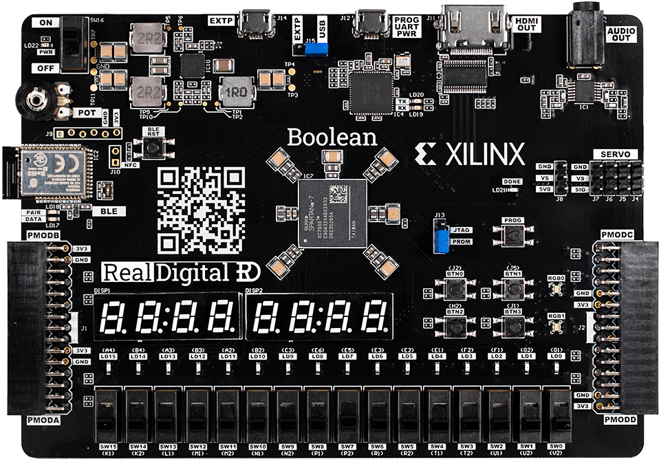
| Spartan 7 Boolean Board
The Boolean board is an FPGA-based educational platform designed specifically for electrical and computer engineering education. Based on an AMD Spartan-7 FPGA, the Boolean board includes a large collection of peripheral devices and ports, allowing countless designs to be built without the need for any other components. The free Vivado CAD tool from AMD can be used for Verilog or VHDL entry, as well as for simulation, synthesis, and FPGA programming. A single USB connection provides power, a UART/COM port, and a programming port. | Boolean Board Reference Manual
FeaturesThe Boolean board is a configurable digital logic system designed specifically for teaching and learning digital logic design.The board is centered on a Xilinx Spartan-7 FPGA (XC7S50) that can be configured into a virtually unlimited number of hardware circuits.The Spartan-7 FPGA includes:
The Boolean board surrounds the FPGA chip with several peripheral devices, including push buttons, slide switches, discrete and RGB LEDs, an 8-digit seven-segment display, audio and video outputs and an optional Bluetooth radio – everything needed to implement a wide variety of digital circuits and systems without the need for any other components. Two 30-pin expansion connectors, both capable of driving two Pmods as well as custom peripheral boards, provide easy access to an additional 44 FPGA I/O pins.
| 7-Series FPGA Family AMD Spartan-7 Product AdvantageAMD Spartan™ 7 devices, the newest addition to the Cost-Optimized Portfolio, offer exceptional performance per watt, along with small form factor packaging to meet the most stringent requirements. These devices feature a MicroBlaze™ soft processor running over 200 DMIPs with 800 Mb/s DDR3 support built on 28 nm technology. Additionally, Spartan 7 devices offer an integrated ADC, dedicated security features, and Q-grade (-40°C to +125°C) on all commercial devices. These devices are ideally suited for industrial, consumer, and automotive applications including any-to-any connectivity, sensor fusion, and embedded vision. Applications
References
| Boolean Board Useful Links Boolean Board Useful Links Boolean Board Reference Manual |
| Xilinx EDA Tools, Flows & Methodologies | ||
| Vivado Design Suite | Hardware Developer
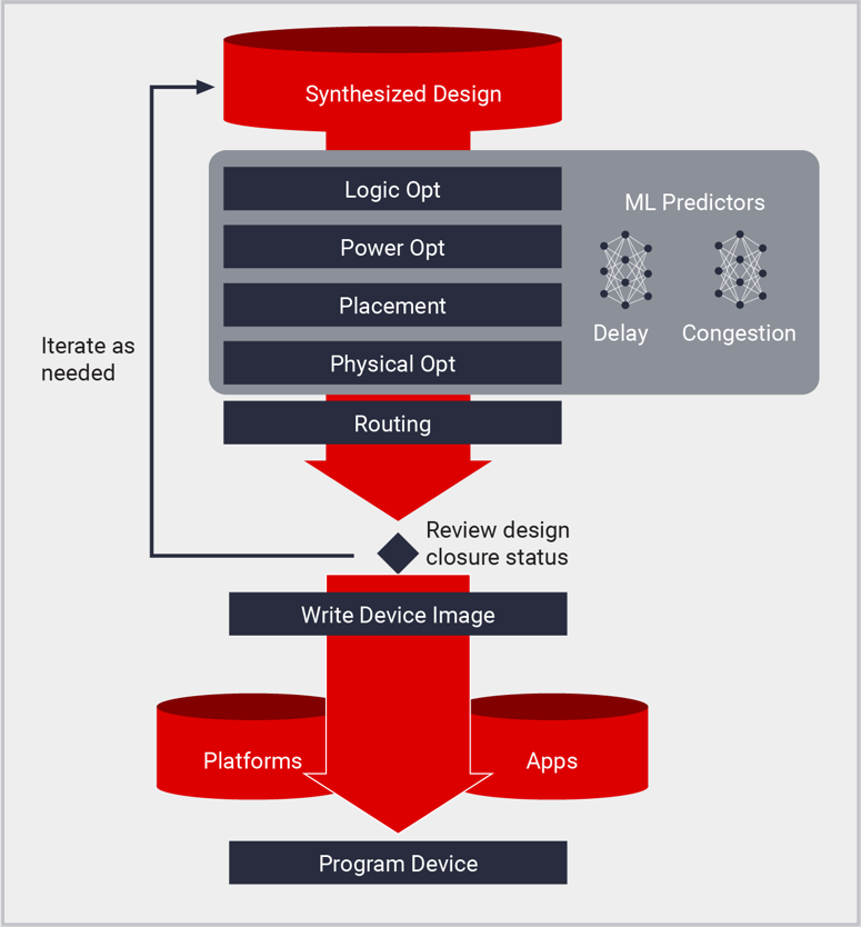
Overview (QuickTake video)Vivado Design Suite is a software suite produced by Xilinx for synthesis and analysis of HDL designs, supersending Xilinx ISE with additional features for System on-a Chip (SoC) develpoment and High-Level Synthesis (HLS). It is an Integrated Design Enviroment (IDE) with system-to-IC level tools built on a shared scalable data model and a common debug enviroment. Vivado includes Electronic System Level (ESL) design tools for synthesising and verifying C-based algorithmic IP, standards based packaging of both algorithmoc and RTL IP for reuse; standard based IP stitching and systems integration of all types of system building blocks; and the verification of blocks and system High-Level DesignVivado IP Integrator provides a graphical and Tcl-based, correct-by construction design development flow. Working at the interface level, design teams can rapidly assemble complex systems that leverage IP created with Vitis™ HLS, Vitis Model Composer, Xilinx IP, Alliance Member IP as well as your own IP. By leveraging the combination of newly improved Vivado IPI and HLS, customers are saving up to 15X in development costs versus an RTL approach. VerificationMeeting the verification challenges of today’s complex devices requires multitudes of tools and technologies at various levels of design. Vivado® Suite delivers these tools and technologies in a cohesive environment for accelerated verification of block- and chip-level designs. | Xilinx Developer Site Whether you are a software developer, hardware developer, or AI scientist, we have you covered with adaptable compute silicon and software platforms to power your innovation
Design HubsDesign Hubs make it easy to learn about specific design tasks by providing introductory material, key concepts, and FAQs along with quick access to the appropriate documentation, videos, and support resources for the task at hand. BoardsFrom concept to production, Xilinx FPGA and SoC boards, System-on-Modules, and Alveo Data Center accelerator cards provide you with hardware platforms to speed your development time, enhance your productivity, and accelerate your time to market. Whether you need an evaluation board to begin development or want to speed time-to-market and lower risk with production data center accelerator cards or System-on-Modules, Xilinx and its ecosystem partners offer the industry’s most comprehensive set of hardware platforms to help speed your time-to-revenue. Intellectual PropertyXilinx and our Partners have a rich library of Intellectual Property (IP), to help you get to market faster. Our IP goes through a vigorous test and validation effort to help you have success the first time. Beyond a simple library of cores we provide other solutions to help your productivity. IP Integrator is a GUI which enables rapid connection of IP which is enabled by a common user interface that is AXI based. This can reduce the design effort by months. We also have IP Subsystems that integrate multiple IP into one solution. Why generate a DMA and PCIe core, when we can deliver an IP Subsystem that does this for you. We have many other Subsystems too. Why worry about peripheral interfaces? Let us help you get to market faster. Focus on your application design. Our IP Solutions are designed to make you more productive.
| Xilinx University Program
The Xilinx University Program (XUP) enables the use of Xilinx FPGA and Zynq SoC tools and technologies for academic teaching and research. Benifits for Students:
|
| Other Generic Usefull Links | ||
| List of FPGAs' Major Manufacturers (Wikipedia)
| List of Electronic Components Distributors (Wikipedia) Findchips offers a single place to view up to date pricing and inventory from the world's largest distributors. Alldatasheet provides semiconductors and electronic component's datasheets for free. | |
| Related/Suggested Course Books A list of related and/or suggested course books. Several are provided by eudoxus platform. | ||
| Related Courses A list of similar related courses provided by our Department. |